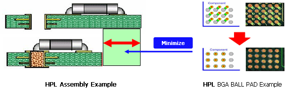
What is ; HPL is VIA ON PAD technique, forming via hole under SMD pad.
HPL feature by structure
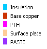
Structure
Feature
Paste
PTH& Surface plating
Non-conductive or radiation
(1.8 ~ 3.0 W/m.k)
PTH plating ellipsis
Conductive or radiation
(1.8 ~ 3.0 W/m.k)
1.2th plating ellipsis, Solderablity
Conductive or Conductive solder radiation
(1.8 ~ 3.0 W/m.k)
Non-solderability
Non-conductive or radiation
(0.8 ~ 2.0 W/m.k)
Effect
Prevent solder bridging between closely spaced holes Eliminate solder flow up via holes during assembly Maximize thermal and electrical conductivity with thermally conductive paste Minimize flux residues and contamination Minimize PCB size and layers Easier to Draw a wiring diagram than normal PTH Prevent micro-chip from slanting while soldering
Copyright 2013 TECHNICOM CO.,LTD. All rights reserved.
Address : B-421, 540, Misa-daero, Hanam-si, Gyeonggi-do, Korea (12925)